Leadtime: 2 to 4 weeks
In-stock alternative to consider: Adapt9S12DP256M2
Product Info
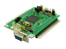
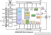
Adapt9S12D is a compact, modular implementation of NXP's 9S12D family of microcontroller chips. Implemented in an "AdaptS12" form factor, the CAN configuration includes all necessary support circuitry for the MCU, as well as a 5-Volt regulator, RS232, and two CAN transceivers on-board (no RS485).
MCU Overview:
Module Features:
- surface-mount 112-pin 9S12DP512 MCU
- 2.30" x 3.25" AdaptS12 form-factor
- two 50-pin connectors bring out all I/O pins of the MCU
- all I/O pins on a 0.1" grid for easy interfacing to standard perfboard
- versatile connector design for use with solderless breadboards, prototyping cards, or embedding into your design
- RS232 transceivers provided for both SCI channels
- two physical-layer high-speed CAN transceivers (PCA82C250 or equivalent)
- 16 MHz crystal, but internal bus can run up to 24MHz (using on-chip PLL)
- accommodates optional user-supplied oscillator
- Background Debug Mode (BDM) fully supported for loading and debugging user code (BDM pod required)
- universal 6-pin/10-pin BDM connectors support BDM pods from multiple vendors
- program in C, BASIC, Forth, assembler, etc.
- no special Flash programming voltage or switch required
- fast in-circuit programming
- on-chip bootloader/monitor (D-Bug12) for quick loading of user programs
- 500mA, automotive grade, low-dropout 5V regulator on-board (underneath)
- includes low-voltage inhibit reset circuit + reset button
- accommodates optional precision voltage reference chip for analog-to-digital
What's included:
- assembled, tested module, pre-programmed with D-Bug12
- red and black power connector cable assembly (#PCJ1-8)
- data sheets, manuals, and all other resources for this product can be found in the Resource Library
Before you order...
Most standard connector options are available for this board (although not all combinations). The product photo above shows "RA1" connector on both H1 and H2. Please make your choice of connectors before adding this item to your shopping cart. Otherwise, the board will be shipped with the default option (no connectors on H1 and H2).
- Flash-based code development using a BDM pod
Use a BDM pod (such as our USBDMLT) to erase and load Flash with your program. The entire 512K Flash can be used for your program.


